-

 作者: martin

Accuphase的AAVA也是直接改Gain,用好久了,現在連綜合擴大機都全用上了。
什是Gain,分享些給門外漢.
-
-
gain=增益
也就是放大倍侓。一般是以dB來計算。
-
-
Dear Leo,
Let's go on with the special BMC technology.
來說說BMC特別的技術
Please understand our basic difference to most of the circuits: We don't use operational amplifier designs for audio, and we don't use any kind of negative global feedback loop for the audio signal. Thus comparing our approach with AAVA or gain cell makes no sense.
請瞭解我們跟大部份線路根本上不同的地方:聲音方面我們不用運算放大設計,聲音訊號也不用任何種類整體負迴授迴圈。因此跟AAVA或是Gain Cell比較是沒意義的。
My last email was about the DIGM. At DIGM we are at the speaker terminal voltage (電壓 ), but there is not the power (電功率) and specifically not the current (電流) to drive a speaker. Thus we need a buffer stage to provide the current.
我上一封Email關於DIGM,在DIGM下,達到喇叭終端的電壓,不是電功率,特別是指不是電流來驅動喇叭,所以我們需要一個緩衝級來提供電流。
In all usual power output stages one pair (or more pairs) of transistors has to handle the signal precision, the voltage and the current. As this is quite demanding, it usually failes in precision - and needs a feedback loop for reducing distortions. There is even the difficulty to handle complex loads, like real world speakers, as they are partly inductive and / or capacitive. This means signal voltage and signal current are not allways in phase. Means: There are moments when the voltage is 0, but there is still a demand for current. How can this be handled by a transistor having the task of caring for the right voltage AND the right current?
在所有一般的功率輸出級,一對或多對的電晶體必須處理Signal precision,就是電壓與電流,且需要回授迴圈來減少失真。處理複雜的阻抗是困擾的,就像喇叭一樣,部份是電感或電容。這意偽著訊號的電壓與訊號的電流通常不是相位一致。也就是說,當電壓為0,但還是對電流有需求,那麼一個電晶體如何處理正確的電壓對應正確的電流?
LEF is different. It is like giving different jobs to different people.
LEF means Load Effect Free. Means: The LEF signal transistor (responsible for the signal quality - the precision) has neather to handle the voltage, nor the current. Thus it needs "assistants": A cascode transistor to handle the voltage changes, plus a pair of current sources to deliver the required current.
LEF是不同的,他將不同的工作給不同的人,LEF意思為Load Effect Free。也就是LEF訊號電晶體(負責訊號的品質- precision)不是處理電壓或電流,他需要"助理",一個cascode電晶體處理電壓的改變,加上一對電壓來源來提供所需的電流。
This circuit design is intended to avoid distortions by a new and unique design, instead of a later correction by feedback.
這樣全新與特別設計的線路用來避免失真,而不是後來回授的修正。
Beside of avoiding distortion, the independend handling of voltage and current by different "experts" makes handling inductive or capacitive loads just a piece of cake: The LEF signal transistor together with the cascode transistor care for the correct voltage. The current servo circuit with the current sources deliver the required current, not "knowing" anything about the voltage, just keeping the current through the LEF signal transistor constant.
除了避免失真外,由不同"專家"獨立的處理電壓與電流,讓處理電感與電容阻抗變成非常容易的事。LEF訊號電晶體與cascode 電晶體共同確認正確的電流。電流伺服線路和電流來源提供了所需的電流,而不用需要知道電壓的狀態,只要保持有足夠的電流到LEF訊號電晶體。
I know, it is difficult to understand, mainly because it is so different from usual amplifier designs.
Best regards,
Michael
-
-
Dear Leo,
Here some more information about LEF. We are often asked, if out design is Class A or AB. As we don't have a traditional design, class A or AB does not really fit. The efficiency is that of Class AB. But the circuit design has nothing to do with Class AB: The LEF signal transistor, that is responsible for the sound quality, works in single-ended Class-A-Mode. But it does not have to handle the change of voltage. As this transistor is supported by a cascode transistor, the voltage over the LEF signal transistor is allways constant, it would be better to call it a "Cascoded Single-Ended Class-A Circuit" - as a first step. There is - as a second step - the current source circuit, separating the signal transistor and the cascode transistor from the current requirement of the load. Should we call it "Cascoded Single-Ended Class-A with Current Relieve Circuit"? (Or "CSECAWCRC"?) Sounds complicated...
針對LEF我再提供多一點資訊,我們通常會被問是A類還是AB類,事實上都不算是,效率可能跟AB類一樣,但線路跟AB類一點也無關。LEF訊號電晶體負責聲音的品質,以單端A類模式運作,但其不負責電壓的處理。當這個電晶體被1個Cascode電晶體所支持著,稱為Cascoded Single-Ended Class-A Circuit比較合適。再來電流來源的線路將訊號電晶體與cascode 電晶體從負載所需的電流分離出來。或是我們要稱之為Cascoded Single-Ended Class-A with Current Relieve Circuit(Or "CSECAWCRC"?),好像很複雜
We think "LEF = Load Effect Free" hits the nail on the head: The signal transistor is free from every effect of the load, free of the voltage swing, and free of the current demand. Because of this reason the LEF signal transistor is free to care for his main task: Reproducing the music signal as best as possible.
LEF恰到好處,訊號電晶體不受到任何負載下的影響,也不受到電壓轉變的影響、也不受到電流需求的影響,也因為這些理由,LEF訊號電晶體可以專心的、達到最佳再生音樂的目的。
As LEF by design avoids distortions, there is no need for a signal feedback loop. This means as well: The LEF stage is independent from a voltage gain stage. (You even could use a tube circuit for the voltage gain and use the LEF circuit as the output buffer...) This independency allows further new circuit designs like the DIGM gain management, as it is explained on page 2.
LEF設計來避免失真,因此就不需要有訊號回授的迴圈,意味著LEF級是與電壓增益級所獨立的 (你甚至可以用真空管線路給電壓增益,然後用LEF線路為輸出緩衝...)這樣的獨立允許進一步的線路設計,如DIGM增益管理,像第2頁提到的
Next time I will explain the CI input circuit.
下一回我將解釋CI輸入線路
Best regards,
Michael
-
-
Dear Leo,
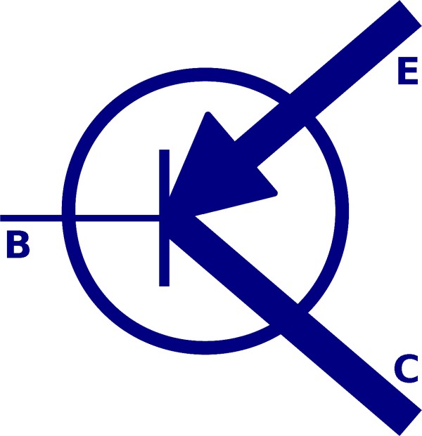
Sorry for delay due to a lot of urgent work! I like to explain more about our CI = Current Injection technology. First let's see how most of the amplfier circuits are working. Please have a look in picture T1. The way of showing this transistor looks a little unusual with a tiny line for B (Base) and much stronger line for C (Collector) and E (Emitter) - but it reflects reality: A tiny signal into B modulates a much bigger current flowing through C and E. We name it: We make a COPY of the incoming signal! And a copy is not the same as the original, always adding some own signature. Same is right for tubes or FETs and MOSFETs. This way some of the characteristic of transistors (or tubes or FETs or MOSFETs) is imprinted to the music signal.
不好意思,最近忙一些,所以有些延遲,我想要進一步解釋 CI = Current Injection 技術。首先我們先來看大部份擴大機運作的方式,請看圖片T1,這圖中電晶體的表達方式跟平常有些不同,B (Base) 的線較細、C (Collector) 與 E (Emitter) 的線較粗,不過這反應了實際的情況,較小的訊號進到C,較大的訊號進到C與E,因此這就是我所們所謂要COPY進來訊號的意思,而這樣的COPY會使得其跟原來的訊號不同,通常會加入自己的東西。這種作法在真空管或FETS與MOSFETS都一樣,而這樣會讓這些電晶體的特性跑到了音樂訊號中。
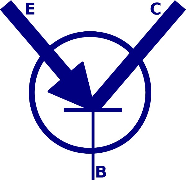
Anyway, making a copy can not be totally avoided. As long as you need more current at the output than you get from your source, there is the need for modulating a higher current by a less powerful signal. At least you need this process for driving speakers. But very often it can be avoided making a copy. How? Have a look at picture T2: The same transistor is turned, B is connected to ground, the music signal is feed into E, and this original current is flowing through the transistor to C. If you could mark the incoming electrons, you could find the same electrons at the output.
不過,COPY訊號是無法完全避免的,只要你在輸出需要比輸入更多的電流,你必須這樣的過程才能驅動喇叭,不過我們卻能避免進行這樣的COPY,要怎麼做?請看圖T2,相同的電晶體,B連接到地,音樂訊號到E,這樣原來的電流就會通過電晶體到C。因此C與E的電子會一樣。(輸入與輸出相同)。
Now let us have a look at a simplified schematic of our AMP M1 or AMP S1 input circuit (picture AMP-CI): The input signal from a source like our DAC1 is flowing through resistor R1 (in this case needed to define the current) and through E and C of the transistor, terminated by resistor R2. The current is same through R1 like through E and C of the transistor and as well through R2. But the voltage depends on the value of R1 and R2: If R1 and R2 are same, the voltage at the input of R1 and the output (C) of the transistor are same. If R2 is only 1/10th of R1, the voltage is 1/10th as well, means an attenuation of 20dB. If R2 is 10 times higher than R1, the voltage is 10 times higher as well, means a gain or amplification of 20dB.
現在我們來看我們AMP M1或AMP S1輸入線路的概要(圖:AMP-CI),從像我們DAC1的訊號輸入通過電阻R1(在這裡要定義電流),然後通過電晶體E與C,最後為電阻R2,這電流與通過R1、電晶體E與C一樣。不過電壓則視R1與R2的值來決定,如果R1與R2一樣,電壓在R1與C會一樣,如國R2只有R1的1/10,則會變小20dB。如果R2比R1高10倍,電壓會高10倍,就是增益或放大20dB。
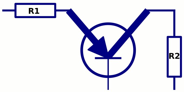
This way we do the gain management (DIGM) of our amplifiers, by changing resistor R2. As this is the only stage for changing the signal voltage in our amplifiers, the output voltage of this stage is the same as the speaker voltage. This means: If you use the CI input of AMP M1 or AMP S1, there is no copy of the original input signal until the speaker voltage is chieved.
Still, at the end we need to drive the speaker. Means: We need much more current than our source can deliver. At this point we need to make a copy, and we do it with our LEF stage. But it means only one copy of the signal received at the CI input.
這就是我們B.M.C.擴大機增益管理(DIGM)的方法,從改變電阻R2來處理。這也是我們擴大機唯一會改變訊號電壓的地方,輸出電壓在這邊是與喇叭電壓一樣的,這意味著,如果你使用AMP M1與AMP S1的CI輸入,直到喇叭電壓,在原來輸入訊號是沒經過COPY的,當然在最終我們仍要驅動喇叭,因此我們需要的電流比我們訊號提供的電流來得更多,因此我們還是需要COPY,但我們在LEF級來處理這部份,這意味在CI輸入下,只有COPY訊號1次。
This is CI explained for amplifiers as used in BMC AMP M1 and AMP S1. The same technology we use for PHONO and DAC as well - explained next time.
這是使用在BMC M1與AMP S1中CI技術的解釋,相同的技術也用在我們的Phono與DAC,我在下次將解釋。
Best regards,
Michael
-
-
Hi Leo,
Thanks a lot for your translation! Today just a short one: CI for D/A-Converter:
Allmost all DACs are based on several current sources 电源 [電源] diànyuán , that are turned on or off. The most significant Bit (MSB) switches the highest current source, the second Bit switches a current source with half the current of the former one, the third Bit switches half the current of the second one, means one forth of the MSB, and every following bit switches a current source that has half of the current compared to the former one. And this for 16 Bit, 24 Bit or 32 Bit (the most common DACs are 16, 24 or 32 Bit). (See picture DAC-CI)
今天要介紹是CI技術在D/A轉換的應用,大部份的DAC以許多電流來源 (電源) 為基礎,電源不是開就是關。最重要的Bit (MSB,most significant Bit) 轉換最高的電流來源,其次的Bit則是只有轉換前面電流的1半、第3個Bit又是只有第2個的1半,也就是只有第1個的1/4,接下來的每個Bit都是依此原則轉換,大部份的DAC大都是16Bit、24Bit、32Bit。

Now these current sources are connected to a CI-circuit, feeding the sum of the switched currents to E of the transistor. At the output the voltage is set by the resistor. At this point there is the output voltage of the DAC, without making a copy. That's it about CI for DAC.
現在這些電流連接到CI線路,提供了全部轉換的電流總合給電晶體E,因此輸出電壓是由電阻決定,在這點這是DAC的輸出電壓,而不需要經過COPY,就這就CI技術在DAC的應用。
Best regards,
Michael


-
-
-
The Following User Says Thank You to drunkenlife For This Useful Post:
-
DAC-CI versus OP-AMP
Hi Leo,
Thanks for your translation again!
Drunkenlife made a nice addition, showing the usual way of I/V conversion by an OP-Amp. Yes, over 99.9% of all D/A-converters use this approach, feeding the DAC current into the negative feedback-loop of an OP-AMP. And the example shown by drunkenlife is for sure one of the better OP-AMP solutions, having only one OP-AMP in each line. Most times there are even more.
感謝你的翻譯,Drunkenlife做了很好的補充,顯示了一般使用OP-AMP進行I/V轉換。是的,有99.9%的DAC都使用這樣的方式,提供DAC店流到OP-AMP的負迴授。drunkenlife所舉例的是其中一個OP-AMP不錯的方案,每一個線路只有一個OP-AMP,一般來說會有更多。
We have a different approach, and we have it for a reason. We don't like overall feedback loops in the audio range. We don't like making COPIES. And OP-AMP-ICs have a limited bandwidth, causing distortions, especially with the unfiltered high frequency trash of the digital domain. From our point of view OP-AMPs can not handle this task without creating distortions. We are sure the frequent complaint of digital sound is the
complaint about the sound of a "tortured" OP-AMP.
B.M.C 有不同的方法,我們不喜歡在聲音的範圍有整體回授,我們不喜歡COPY,OP-AMP-ICs的頻寬有限,會造成失真,特別是數位未經濾波的高頻。我們認為OP-AMPs無法解決這問題而沒有造成失真。我們確定一般抱怨的數位聲就是這裡所產生的。
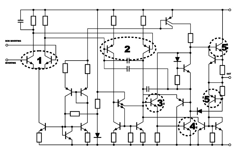
As I explained in post #25, we prefer avoiding copies by using our CI circuit. Attached is a schematic of one of the most used OP-AMP-ICs, the 5532. I have marked all the copy stages. You can see there are 5 copies done with this IC, means at the output you get a copy of a copy of a copy of a copy of a copy of the original input signal - just with one IC. Most circuits use several ICs in series.
在這篇編號#25中我有解釋,我們偏好在我們的CI線路中不要COPY(訊號),這張圖是最常用的OP-AMP-IC之一,5532,我標記了所有的COPY級,你可以看到這個IC有5個COPY地方,意味著在輸出時,你得到的是a copy of a copy of a copy of a copy of a copy of原來的訊號,且發生在只有一顆IC上,大部份的線路又使用了許多的IC。
OP-AMP-ICs only can be used with an overall negative feedback-loop, otherwise distortions and gain are too high and frequency response is decreasing a lot in the audio range. Due to the decreasing frequency response the phase is changed as well. All OP-AMP-ICs used for audio have a phase turned by 90?over most of the audio range. That is not ideal for a feedback-loop... I could go on with OP-AMP-IC-bashing some more pages... But just take it as our reason for a different circuit design without any need for overall negative feedback.
OP-AMP-ICs使能使用在整體負迴授,不然失真與增益會過高,頻率響應會在聲音範圍減少很多。由於頻率響應的減少,相位也會改變。對迴授這不是非常理想的方式。我可以說更多有關OP-AMP-IC-bashing,不過我只想說明這是為什麼B.M.C採用不同的線路設計,且不需要整體負迴授。
Thus we use a different approach, feeding the original current of the DAC chip into E (emitter) of the transistor and using this original current, until we define the output voltage with a resistor. At the output we still need a small LEF buffer for driving cables and following loads. But this means we make just one single copy.
因此我們用不同的方法,給DAC晶片原來的電流到電晶體的E(emitter),使用原來的電流,直到我們在電阻來確定輸出的電壓。在輸出我們依然需要LEF緩衝來驅動線材與阻抗。不過這意味我們只需一個單一的COPY。
Please keep in mind: Our shown circuits are kept simple for explanation.
Reality is more complex.
請記得這裡舉例是經過簡化的,主要為了解說方便,B.M.C的線路實際上是複雜很多的
Best Regards,
Michael
-
-
小葉,這一句“I could go on with OP-AMP-IC-bashing some more pages”是說,“如果我想要的話,我可以寫好幾頁OP-AMP-IC的壞話”。
另外,電晶體的三極:
E(Emitter): 射極
B (Base):基極
C (Collector): 集極
-
The Following 2 Users Say Thank You to kevintran For This Useful Post:
-
-
 發文規則
發文規則
- 您不可以發表新主題
- 您不可以發表回覆
- 您不可以上傳附件
- 您不可以編輯自己的文章
-
討論區規則
|